Continue to Site

Welcome to EDAboard.com

Welcome to our site! EDAboard.com is an international Electronics Discussion Forum focused on EDA software, circuits, schematics, books, theory, papers, asic, pld, 8051, DSP, Network, RF, Analog Design, PCB, Service Manuals... and a whole lot more! To participate you need to register. Registration is free. Click here to register now.

how single nmos/pmos Directly go to saturation

Status
Not open for further replies.

sunnymeharwal

Newbie level 4
Newbie level 4
Joined
Sep 15, 2008
Messages
6
Helped
0
Reputation
0
Reaction score
0
Trophy points
1,281
Visit site
Activity points
1,349
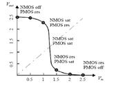
From CMOS Inverter voltage transfer characteristics, we see that nMOS transistor switches from Cut-Off (region - A ) to Saturation (region - B )
and pMOS transistor switches from Saturation (region - D ) to Cut-Off (region - E ).

This can be explained by equations and by calculating the Vds which satisfies the above conditions.

But nMOS and pMOS transistors are practical devices,
So, in case of switching of nMOS from Cut-Off (region - A ) to Saturation (region - B ) the linear region should come in between.

Is the linear region comes in between or
nMOS does not enter into linear region even for a very short interval of time ?

Thanks[/b]
 

consider a cmos inverter.when it is off i,e at vin=0 the pmos can be replaced by a resister connected to a cap i,e it is in resistive(linear) region. Nmos is off
when vin is increased then the nmos can be replaced by a current source i,e it enters saturaion and pmos is still resistive

on further increase nmos and pmos both saturate and pwr dissipation is maximun

next nmos turns resistive and pmos is in saturation. when vin reaches Vdd nmos is in replaced by resistor and pmos by open circuit
 

Hi,
What balavinayagam says is correct,
but there is another thing to consider in a general analysis.
For the transistor to exit cutoff region Vgs-Vth must be > 0.
When this happens some people assume it goes in to the linear region,
because this is how the I-V curve goes. This is not always true.
Consider for a moment a common source amplifier with a PMOS load.
Lets say for a moment that Vin=0, where Vin=Vgs=Vg (since the source is grounded) and the capacitive load at the output is now charged to Vdd.
When we exit the cutoff region Vds>Vgs-Vth and we go right in to saturation!
Acctually, this happens in most analog applications. Linear region is used more in digital applications.

Thats my 2 cents.
Hope this helped you in some way.
 

Thanks for explanations....

Please take the case of single MOS Transistor...
my actual question is that when we fix Vds at max. Vdd suppose..... and increase Vg from 0 to Vdd...NMOS first inter into the saturation when Vg>= Vt. Equation satisfies these things...even transfer Characteristics. But my question is how it is possible for a device to directly go to saturation WITHOUT GOING TO LINEAR.. physically how thins happens....i m still confused. hope u understand my question. Please take the physical and qualitative analysis of a single MOS transistor into consideration.
 

Oh... I see.
Ok. Two different answers then.
First the quantitive. As I said before. A single NMOS is connected to Vdd (Lets say it`s 2.5V) at the drain and GND on the source. Now, We start sweeping the gate voltage from 0 to Vdd.
Vgs-Vth becomes larger. Lets pick a value, lets say Vgs-Vth=0.2V,
now check Vds=2.5V and Vgs-Vth=0.2V. Vds>Vgs-Vth. So we are in the saturation region! (This is of course theoretic, since this type of connection is pointless).

Now for some physics. You know how a channel forms with an inverted carrier population under the gate? When Vds is much larger than Vgs-Vth, the electric field at the drain side is so strong that the channel does not completly reach the drain. Since the electrons must still travel from the source to the drain, the part where the channel isn`t fully formed accelerates them. This is why saturation current is much stronger than linear current. By the time the gate voltage is large enough, the channel is already formed. This is called channel pinch off.

Hope this was better :D
 

When the transistor exits sub-threshold, which mode it goes into depends solely on how its vds compares with its overdrive. There is no constraint on what it's overdrive should be, besides the fact that it must be positive!

From a physics point of view, as gate voltage increases, the channel is formed right from the start with a pinch-off, hence transition from cut-off to saturation! A uniform channel will only be formed for zero (or small) vds, ie linear mode!
 

means from device physics point of view... number of electrons (in NMOS) in the channel will be maximum in the initial stage itself(when we increase Vgs from or just at Vt at Vds be Vdd). but how it is possible... i mean population of electron should go from min. to saturation gradually. But we are saying directly saturation condition. is this ok?.... from physics point of view.
 

Well acctually saturation is not the max number of electrons in the channel.
It`s just the fastest moving.
From gate to bulk there is a capacitance, and as with any capacitor, the higher the voltage on one plate, the higher it is on the other plate, i.e. when Vgs is maximum, electrons in the channel are at maximum and this happens in the linear region.

In saturation, the channel is not completlly formed on the drain side, this is called pinch-off. Pinch-off causes Vd (drift velocitiy) to become larger. The lack of a large number of electrons, also helps speed.

On the other hand in the linear region there is a large number of electrons in the channel and Vd is much smaller:
a. because the channel is fully formed and there is no pinch-off acceleration.
b. The mean time between collisions becomes smaller, because of the large number of electrons in the channel.

The reason it`s called saturation is not because the channel is saturated with electrons, the name is historic. Comes from BJT.

This is also why Id is constant (almost) in the saturation region in respect to Vgs.
Because Vgs is not the main component in controlling electron movment in saturation.

If you want to go deeper than this, I advise reading "Operation and modeling of the MOS transistor" by Yannis Tsividis.

I think it`s more or less the best and most comlete book you can find on the subject.
Everything you ever wanted to know and a whole lot of stuff you didn`t :)
 

Checkmate said it. If Vds > Vgs-Vt for all cases there is no transition through linear region. The channel is always pinched off.

The mosfet never enters cut-off either. The operating point transitions down the family of curves on a fixed Vds until current stops flowing. It is in saturation with 0 Id.

A source follower is always in saturation.
 

thanks a lot of u people for sharing your views..... i will still dig these topics further... if there will be doubts ..i will further put my queries
 

I didn't go thru all of your answers fully but the answer to the original question is:

Imagine a switch connected is between a capacitor and a battery. when you swicth ON, the cap charges to Vmax of the battery. To reach a steady state it requires some time. The time duration is because of the series resistance of the battery and time to charge the plates of the capcitor.

Now same thing happens when you suddenly switch ON the gate voltage of an NMOS transistor. But all this happens quickly, so that gates voltage charged to Vg. That is why we are biasing the transistors so that the transistor directly goes to the operating point based on your biasing.

Transistor operating regions are only to understand exactly what happens at different voltages (Vg and Vd), so don't have to worry how many regions it crosses.

Hope this helps

Added after 32 minutes:

yes, it crosses Linear Region to go Saturation before reaching the steady state. But the transistor is almost small as atom,so the gate cap won't take much time to charge.
 

yru... can you please give some documental proof of your views... i have discussed with few experts.. but none has satisfied me with proper answer and proof...
Things are not getting cleared but ..getting confused..bcz no book mention this thing how the single mos transistor directly (or through linear)go to saturation. Everyone gives views but no proof.... pls make this clear..it is very basic and important concept of MOS device physics ..but no confident answer


One view was given by Eladla that number of electrons in Channel in saturation is small in comparison to linear region of nMOS transistor...what is the proof....what is the physics behind it ...can anyone explain
 

The definition of saturation is Vds > Vgs - Vt. If the circuit never violates this, the transistors are always in saturation. Current can flow from drain to source whether in saturation or in linear mode.

I do not understand what other proof you want.
 

equationwise , everything is correct. but my question is ..Please take the case of single MOS Transistor...let us take nMOS

when we fix Vds at max. (Vdd) suppose..... and increase Vg from 0 to Vdd...NMOS first inter into the saturation when Vg>= Vt. Equation satisfies these things... i know..even transfer Characteristics. But my question is how it is possible for a device to directly go FROM CUT OFF TO SATURATION. WITHOUT GOING TO LINEAR REGION.. i WANT EXPLANATION FROM DEVICE PHYSICS POINT OF VIEW. if a device goes directly from cut-off to saturation...then it is the ideal case.
. but nothing is ideal. Can u explain this. just forget Equations mentioned in the books...and think from device physics point of view.
 

Okay I see.

In NMOS linear operation, there is a low resistance channel of electrons attracted to the surface near the gate, which connects the n-type source to the n-type drain. To form this channel, the body surface near the gate must be enhanced by a positive gate voltage which attracts the electrons to the surface.

The Vds applied to this channel drops across it linearly with distance to the source, just as any voltage dropped across a resistor varies linearly with distance.

Let Vds=2,Vgs=2, Vt=1 Assume Vds drops linearly across the body from drain to source. At a point roughly half way between drain and source, there will be no channel formed because the voltage at that point =1V and Vgs-Vt=1V. There is 1V at that point due to Vds. The differential voltage between the gate voltage applied (=2V) and this voltage point on the body (=1V) is 1V and it requires at least 1V to overcome Vt=1V and start channel formation. From that point up to the the drain there is actually negative voltage from the gate to the body.

Now consider the situation where Vds is always high and Vgs=0. This pinchoff point starts at the source and moves towards the drain as Vgs increases but it never reaches the drain. The mosfet is always in saturation. There never was a case where a complete resistive channel existed between drain and source.
 

@ sunnymeharwal

I think you're over engineering a simple concept. Don't think about equations, basically a trasnistor will not jump directly from cutt off - sat or vice versa and no circuit/systems can't jump this is very basic. Don't forget that circuits has to go thru the instaneous values. At any point of time there can be only one node voltage in the circuit. For example, If apply a DC voltage of 5V to a circuit and suddenly switch to 10V. doesn't mean magically goes to ten, it raises up to 10 crossing 6, 7,8 9 and reach 10 volts thru the capcitor. I don't think this will be explained in any book, as this evident to an engineer.

If you still don't undertstand i can provide you a picture explaning.
 

@yru

Don't think about equations, basically a trasnistor will not jump directly from cutt off - sat

The thing is... when you don`t think about equations is when you make mistakes like thinking the transistor doesn`t go from cut-off to saturation. You see, if you look at the equations you will see that is exactly what happens, and if you want to go a little deeper, you can check out a more detailed transistor physical model, and then you will also understand why that is. Even in sub-threshold the Id curve is more like saturation than linear, so how could it go right in to linear out of cut-off. It all depends on Vds. You`re just confusing people.
 

Hello eladla

There is nothing to confuse here, the orginigal question how does the transistor go to saturation from cutt off, you can explain with equations. The person who asked the question have understood the equations and he/she doesn't want to explain thru equations. Very simple I will rephrase the quetsion, this is my undertsnading from the original question. In a stairs how do you move steps. definitely you can keep one leg on step 1 and 2nd leg on stair 10. you need go in steps. NO way a circuit system jumps discreetly. I think I have answered his question not to confuse anyone.

---------- Post added at 09:45 PM ---------- Previous post was at 09:40 PM ----------

further to your statement
Even in sub-threshold the Id curve is more like saturation than linear, so how could it go right in to linear out of cut-off. It all depends on Vds. You`re just confusing people.

we are not talking about diff regions of transistor and neither I am talking about it. I am only explaining how voltages on a node (e.g vg). Doesn't what is vg, vd or vs. All I am saying is what ever the combinations it the transistor will react to the instantenous terminal (vg, vd, vs) values and therefore it will cross the regions based on the inputs. I don't see any confusions here.

---------- Post added at 09:49 PM ---------- Previous post was at 09:45 PM ----------

corrections
we are not talking about diff regions of transistor and neither I am talking about it. I am only explaining how voltages on a node (e.g vg) changes. In other words, what ever the combinations of vg, vs, vd the transistor will react to the instantenous terminal (vg, vd, vs) values and therefore it will cross the regions based on the inputs. I don't see any confusions here.
 

Here's a *hopefully* idiot-proof version. Balance 2 ants on a see-saw. The see-saw does not tilt due to friction. This does not imply the see-saw is balanced!. Keep adding an ant to one side until the see-saw tilts. There you have it! Direct transition from cut-off to saturation.
As I mentioned before, the assymetrical channel is formed even during cut-off, it's just that the carriers do not have enough energy to cross the channel! Your problem is that you are too engrossed in the Id-Vds graph. Go figure which operating mode is the transistor at the origin.
 

Status
Not open for further replies.

Part and Inventory Search

Welcome to EDABoard.com

Sponsor

Back
Top