Continue to Site

Welcome to EDAboard.com

Welcome to our site! EDAboard.com is an international Electronics Discussion Forum focused on EDA software, circuits, schematics, books, theory, papers, asic, pld, 8051, DSP, Network, RF, Analog Design, PCB, Service Manuals... and a whole lot more! To participate you need to register. Registration is free. Click here to register now.

folded cascode biasing ........??

Status
Not open for further replies.

ASHUTOSH RANE

Member level 2
Member level 2
Joined
Aug 7, 2009
Messages
49
Helped
2
Reputation
4
Reaction score
1
Trophy points
1,288
Location
KOZICODE
Activity points
1,589
HELLO GUYS
PLEASE TELL ME HOW TO GENERATE BIAS FOR Vb1 and Vb2

i have attached pic
 

Hi, ASHUTOSH RANE
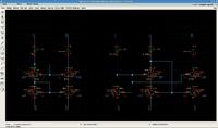
Two examples of biasing nmos are depicted on the picture below:

The first way (left current source on the picture ) is the most simple way if you have enough voltage headroom. And the second way (right current source on the picture) lets you increase the dynamic output voltage range at the cost of drop in output resistance.The width of transistor N11 is 9 times less than that of other transistors in this example. You can vary this parameter and see how the picture of output resistance vs. output voltage changes and choose appropriate value.
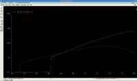
Small signal output resistances are on the figure below:

Regards, pavel.
 

Status
Not open for further replies.

Part and Inventory Search

Welcome to EDABoard.com

Sponsor

Back
Top