Continue to Site

Welcome to EDAboard.com

Welcome to our site! EDAboard.com is an international Electronics Discussion Forum focused on EDA software, circuits, schematics, books, theory, papers, asic, pld, 8051, DSP, Network, RF, Analog Design, PCB, Service Manuals... and a whole lot more! To participate you need to register. Registration is free. Click here to register now.

Altium: Printing pcb for etching with holes in pads.

Status
Not open for further replies.

steinar96

Member level 5
Member level 5
Joined
Oct 9, 2009
Messages
94
Helped
24
Reputation
48
Reaction score
24
Trophy points
1,288
Visit site
Activity points
1,989
Hello, i'm trying to print a pcb layout for etching at home in altium designer. There is one huge annoyance however which is that pads are printed as solid black instead with holes in it (when printing gerber output)

The holes are quite important because if not present, the drilling will tend to get very inaccurate because the drill has a hard time penetrating the copper (it will skip around on the surface if not carefull which means odds are that once it penetrates the copper properly it wont be in the right spot). By etching the pads with holes in it this proplem is eliminated.

Does anyone know how to configure alitum to leave holes when importing the gerber files. The holes need to be present when i print the bottom/top layouts.

any help would be greatly appreciated.
 

Hi,
Try to use File -> Print preview instead of Gerber if you have the pcb file.

Gerber files doesn't produce hole information and NC Drill files is used for this purpose.

Nishal
 

Every PCB tools has means to achieve want you want. Some layout editors as Cadstar have annular pads. Altium hasn't, but you can edit the aperture table in the Camtastic gerber tool and replace round pads with "donut" respectively square with "square donut". Other gerber tools should have similar options.
 

FvM....actually i've tried that, but unfortunately nothing changes in the shematic. But i think i've found a workaround which involves printing it to a image with a virtual printer driver which exports it as a image. Then use photoshop to add the holes. The proplem with that is it gets scaled. So i have to manually rescale it to be correct again. I still have to find out by what factor i need to rescale the done work to make it correct again.
 

if you use all pads and vias on the bottom layer then you can print your pcb with holes in print preview.i am using this tech in protel 99se.
 

Has anyone found a better solution to this with Altium (Summer 09)? Editing apertures somewhat works, you get the donut pads but then can see the connected trace ending in the middle of the donut.
(I realize this is an old topic, but it doesn't seem to have been solved or discussed anywhere else on the forum).

Edit: as it happens so often, right after posting you find a hint to the solution. :)
Print preview instead of Gerber seems to put holes in the pads, just make sure Holes is checked in the print configuration. Sigh, this would have saved me so much trouble knowing before etching...
 
Last edited:

I admire your industriousness... but I have trouble understanding why anyone would etch their own boards. For very little money you can have high-quality prototype PCBs made which have plated-through holes, soldermasks, and silkscreens. Just Google "PCB Prototype". Most PCB vendors aren't looking for hobbyist business but some are willing to take it. Advanced Circuits, Olimex, Silver Circuits come to mind (I haven't used them but they look like good alternatives to making your own, and it's their specialty so the quality has got to be a lot higher than anything you could do yourself.)
 

I admire your industriousness... but I have trouble understanding why anyone would etch their own boards. For very little money you can have high-quality prototype PCBs made which have plated-through holes, soldermasks, and silkscreens. Just Google "PCB Prototype". Most PCB vendors aren't looking for hobbyist business but some are willing to take it. Advanced Circuits, Olimex, Silver Circuits come to mind (I haven't used them but they look like good alternatives to making your own, and it's their specialty so the quality has got to be a lot higher than anything you could do yourself.)

There's always the DIY factor - it may not be perfect, or optimal, but the satisfaction of having it done yourself should be experienced at least a few times to be appreciated.

Regardless of that, I do have additional, perhaps more valid reasons:
For one, since we're talking prototypes, perfect quality is not even remotely an issue. "Good enough" is rather what I'm looking for, as a tradeoff for fast and cheap.
The cheapest good quality PCB house I know of (ExpressPCB I believe) will still take $70-$100 and a few days for a 3x3 inch board (or twice the money for overnight shipping). And, if you realize you need to make changes to your board, the cost and time go up quickly.
While money may not be an issue (it is), time is definitely a factor. Most of my hobby time is over the weekend, since I'm too busy working Mo-Fr, so that would mean I'd need at least one week between sending off a board to the PCB house and getting to work with it.

As far as efficiency for at-home etching, it has become very simple and fairly accurate: print your layout using a laser printer and your favorite transfer medium (I use pulsarprofx), transfer (laminate) it to the board, etch, clean with acetone, drill holes and populate. Repeatable down to around 5 mil traces matched on a double sided layout, I'd say that's enough precision for any home project. :)
 
Thanks, I didn't know about pulsarprofx... the last time I made my own PCB was a really long time ago, I had to use photosensitive materials. The time savings is definitely a big plus. My boards are all destined for production so I'll still keep using PCB vendors, but maybe I'll try it sometime if I need a one-off.
 

It is possible to show holes . i did it with sigle and multilayer pcb . U HAV TO GENRATE PDF. NOT POSTSCRIPT . FORGET GERBER . IT IS POSSIBLE WITH GERBER TOO . FIRST ADD OUTPUT DOC. IN THAT SELECT ONLY MULTILAYER TOP LAYER AND KEEPOUT . WITH THIS TICK ON TOP SIDE AND HOLES. SEE THE PRINT PREVIEW . ULL GET HOLES . THIS IS OK PDF ONLY . IF U TRY TO GET POST SCRIPT FILE FROM THIS ULL GET AND PS FILE WITH SOME PADS VIAS MISSING . FROM PDF U CAN MAKE FILMS ONE BYE ONE .

ANOTHER OPTION IS FROM GERBER .

1. GENRATE GERBER ALONG WITH NC DRILL FILE
2. USE GERB TOOL 12 SOFTWARE
3. IN THET LOAD FIRST GERBER FILES .
4. EXPORT EACH LAYER TO POSTSCRIPT
5. CLOSE CURRENT SESSION OF GERB TOOL
6. OPEN NEW - IMPORT NC DRIL FILE.
7. EXPORT IT TO PS
8. OPEN CORAL DRAW 11
9. IMPORT ALL PS FILES.
10. MATCH NCDRILL PS FILE WITH ONE OF TOP OR BOTTOM LAYER

NC DRILL PS FILE CONTAINS ACTUAL HOLE SIZE FILE .
I HAV TRIED THIS PROCEDURE SUCCESFULLY.
IT WORKS.
 

Thanks, I didn't know about pulsarprofx... the last time I made my own PCB was a really long time ago, I had to use photosensitive materials. The time savings is definitely a big plus. My boards are all destined for production so I'll still keep using PCB vendors, but maybe I'll try it sometime if I need a one-off.

Yes, production is an entirely different animal. :)

If you ever try getting back into it, be warned that you'll have a one-time "tooling" cost (getting transfer paper, making sure you have a laser printer, laminator, drill press and etching materials).

The least controllable step in all this is the etching, I think. It's easy to overetch and lose some continuity.
And, in retrospect, I wouldn't do vias under surface mount components again. It's a painful thing to get the surface flat enough. :-|

Also, if you do PCBs regularly, you can get a particular Epson inkjet printer and a **broken link removed** for it, so you can print your layout directly on the board. That eliminates the need for transfer paper and laminating. For me it isn't worth it, the printer would dry out at the rate I'm making boards at... :lol:
 

Hi Guys,
I think this might be the solution you are looking for:

To print holes on your PCB artwork
File -> Default Prints
1. Set PCB Prints as your default print
2. Configure PCB print
3. In the "Printout Options" column tick "Holes"

4. Change your printing preferances to mono, this step will print the holes as white instead of grey.

5. Print in the normal fashion

Hope this helps :grin:
 

the exact solution is
first from pcb editor ->fabrication outputs-> nc drill
then from generetad cam file, fabrication output ->gerber ->save as rs-274-x
goto pcb editor ->fabrication outputs-> gerber
from generetad cam file import the previos gerber drill file(select all files as filter) drilled.png

- - - Updated - - -

the exact solution is
first from pcb editor ->fabrication outputs-> nc drill
then from generetad cam file, fabrication output ->gerber ->save as rs-274-x
goto pcb editor ->fabrication outputs-> gerber
from generetad cam file import the previos gerber drill file(select all files as filter)drilled.png
 

    V

    Points: 2
    Helpful Answer Positive Rating
After a few hours of head scratching, I just found the right solution :)
Repeat steps described by anil01, realign layers if is necessary (Edit->Layers->Align Selective, click on some pad and after this click on the corresponding drill).
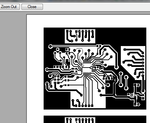
Panelize if needed. Change layers color - tracks in black and drills in white . Before print, select from print dialog - "Print color: color". Print :)
Here is the result - print.png
 
Dylan Owen's method is working fine for me. Just make sure you choose Hole in the Default Prints-Fabrication outputs if you are going to use that. The weird thing is that the print out on bottom layer of my design come with some sort of over lapping with one of the silk print (mechanical layer). have to end up un-tick them all. anyway, check carefully before you put onto the board. ps: Adobe Illustrator is really handy to take the pdf directly and flip into one page.
 

Status
Not open for further replies.

Part and Inventory Search

Welcome to EDABoard.com

Sponsor

Back
Top