Continue to Site

Welcome to EDAboard.com

Welcome to our site! EDAboard.com is an international Electronics Discussion Forum focused on EDA software, circuits, schematics, books, theory, papers, asic, pld, 8051, DSP, Network, RF, Analog Design, PCB, Service Manuals... and a whole lot more! To participate you need to register. Registration is free. Click here to register now.

Adaptive biasing of source degeneration mos

Status
Not open for further replies.

simplsoft

Full Member level 2
Full Member level 2
Joined
Nov 24, 2014
Messages
127
Helped
0
Reputation
0
Reaction score
0
Trophy points
16
Visit site
Activity points
1,045
Hello

I am designing an OTA with improved linearity and I have used source degeneration technique and the source degeneration is a MOS resistor operating in triode region. I dont know how to adaptively bias the gate voltage of the triode MOS(source degenerated). The OTA is operated in sub-threshold region except the source degenerated MOS. Can anyone help me in adaptively bias the gate of the source degenerated MOS.

If I fix the gate voltage of triode MOS then the source and drain voltage will vary due to which the linearity will vary thats why I have to use adaptive biasing

Thanx
 

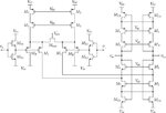
Please find the attached diagram.

The Mtun is the circuit need a gate voltage. How can I adaptively bias the Mtun transistor which is the source degeneration MOS.

Thanks

image-1.jpg
 
Last edited:

Why do you need the Mn transistors? Those are reducing the Gm of the diff. pair (M1 transistors). If the voltage gain of the diff. pair is not enough high, than under control the vds variation of the Mtun tuning transistor will be high, and the device won't operate in deep triode region.
Also, the input inverters are necessary? Those gain variation is really high over process, voltage, temperature and only in a small domain will be linear.
Why did you connect all Mc1,Mc2,Mc4,Mc4 into diode?
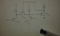
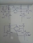
If you can maintain that the vds variation of Mtun is low enough, you can use source follower to create gate voltage for Mtun, like this:

Here the common mode input voltage variation doesn't cause problem, the gate voltage of Mtun follows it by the source follower.
 

Can you elaborate this bit:

the gate voltage of Mtun follows it by the source follower.

Best
 

If the common mode input voltage changes, the gate voltage of the Mtun will change with it.
The source follower's Vgs is equal with the Vgs of Mtun, so it guarantees a Vgs for Mtun which is independent from the common mode input voltage, and keeps constant the ON resistance of Mtun.
 

Thanx for your reply. I am using Mtun transstor to linearize the OTA and Mtun is operated in triode region to work as resistor

- - - Updated - - -

Thankyou for your reply. I think one more common drain amplifier will should be used on the left of the ckt. i.e with the source of MN tranistor. What I have understand is if the gate voltage of MN' increases the source voltage will also increase and the dran voltage of Mtun ill increase simultaneously the gate voltage of M2 will increase and source voltage 0f M2 decreases whicha lso decreases the gate voltage of Mtun which will decrease the increase voltage at the source of MN'. but the same should happen on the MN side too.? I think so. What do you think ?
 

You are welcome. But I still think it won't be very linear with the inverters on the input. And if you connect all transistors into diode at the output it won't help also on linearity, and current variation will be high in the output stage.
 

Thanks for your reply. If I use the circuit like this in attached schematic. I m concerned with the Mtun transistor. This circuit you have attached is a negative current feedback circuit. Am I right? In my opinion the source voltage of MN transistor should also be controlled.
Actually its a bit confusing hope you can help.
pic1.jpg
 

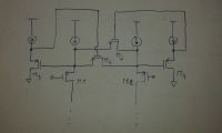
My guess is it doesn't matter too much if you use the source of MN to generate a control voltage for Mtun, because if the source voltages of MN and MN' are quite close to each other, than Mtun will stay in deep triode region. It will be possible if the diff. pair's input voltage difference is low enough (max. 100mV). Depends on application. If you worry about the high variation of ON resistance for Mtun, you can minimize change of the resistance range between Ron/2 and Ron for Mtun with this modification:


But the vds variation of M5 and M6 is not eliminated so maybe it doesn't help I think. It is just more symmetric...sorry.
...and what is confusing hope?
 
Last edited:

If the vds variation of M5 and M6 is not eliminating then it means the Ron will vary which will vary the transconductance of the circuit. Linearity will not improve.
 

yes. it just keeps constant the Vgs voltages, which helps on linearity. but use resistor instead of MOS, than vds variation will be solved.
 

Thanks for your reply. I am using MOS transistor in place of a resistor because resistor occupies larger area. What if I connect two series Mtun transistors and two negative feedback common source transistors.
 

The problem of MOS resistor is you can't eliminate vds variation. I think it is almost impossible, doesn't matter how you create biasing for it.
The source voltages of the diff. pair's transistors never will be equal, then the resistance of the MOS resistor always increase. Same happens with two series MOS, the ON resistance will increase with different source voltages.
Are you sure the area of one resistor is too high? The most linear device is the resistor in a CMOS process, doesn't require bias circuit, extra current.
 

In most of the research article MOS is used in place of resistor then how do they linearize the differential amplifier the biasing circuity is not shown in research articles. I m attaching one schematic I think there must be some improvement in this circuit.
double.png
 

Keep articles with cautious, first suggestion.

Second, you can connect any control to that middle node, I just can repeat myself, to keep vds at zero for both transistors is impossible in this case too. Because the source voltages of the diff. pair won't be the same if you control them with differential voltage. Just the effect of common mode input voltage can be eliminated with the added source followers.

For example, you pull down Vin-, pull up Vin+:
-> MN source voltage decreased, the Vg of Mtun follows it by the left source follower -> Vgs of MN doesn't change, but Vds on MN is increased -> Ron of Mtun is increased

Now you try to compensate with a lower voltage between the 2 series transistor the effect of Vds increasing on Mtun, what happens:
-> Vgs and Vds of MN is the same as before -> the Vds of Mtun' is doubled -> Ron of Mtun' is icreased more than x2!

Actually, do you know how much will be the maximum differential input voltage of your circuit? If it is less than 100mV I am sure you can use my last topology. It should be quite linear for lower differential input voltages, and common mode is not a problem.

- - - Updated - - -

Something just got into my mind, but I am suspicious about it:
https://obrazki.elektroda.pl/3040699200_1510947998.jpg
In this case the common mode problem is solved, and the input differential voltage maybe has got less effect. I am not sure, just an idea.
 

This is stillsome problem with the circuit. I think there is some body effect issue.
 

Thank you for your help. Can you please tell me whats the difference between both circuits. Is there any advantage of adding source followers?

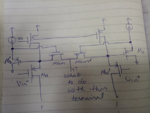
IMG-20171125-WA0002.jpg
 

I think I wanted to draw NMOS transistor for Mtun, but actually you are right, source followers in the lower figure are not necessary.
 

Status
Not open for further replies.

Part and Inventory Search

Welcome to EDABoard.com

Sponsor

Back
Top