Continue to Site

Welcome to EDAboard.com

Welcome to our site! EDAboard.com is an international Electronics Discussion Forum focused on EDA software, circuits, schematics, books, theory, papers, asic, pld, 8051, DSP, Network, RF, Analog Design, PCB, Service Manuals... and a whole lot more! To participate you need to register. Registration is free. Click here to register now.

3 level NPC inverter with UCC21521 gate driver with bootstrap

Status
Not open for further replies.

kaanaydin

Junior Member level 1
Joined
Aug 28, 2017
Messages
19
Helped
0
Reputation
0
Reaction score
0
Trophy points
1
Visit site
Activity points
144
Hi everyone,
I have some problems with 3 level npc inverter topology. When I tried the same circuit with 2 level full bridge,my results were excellent but when I tried with 3 level NPC, NOTHING. Btw I am using spwm for driving.

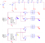
I will share my circuits and output voltage, I'm using ti UCC21521 dual high/high,low/low,half bridge driver for driving. Also my mosfet is SCT3160KL SiC mosfet. Don't forget all circuit is working with 2 level, I have no problems with models.

But I think the main problem is that ground level. Gate driver IC is not firing sicmosfet gates because of the ground level :oops:


I am waiting your suggestions.

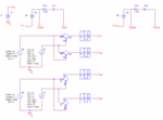
first page.PNGspwm.PNGsecondpage.PNG

- - - Updated - - -

btw ; the bootstrap capacitors inital charged. I dont need to first charging circuit for them
 

U6 VDDB is connected to +25 V and U6 VSSB is connected to -600V. This makes 625 Volt on VDDB-VSSB, but on the datasheet maximum VDDB-VSSB is 30 V. Also you have "chained" or series connected bootstrap supplies VDDA and VDDA2 which reduces driver voltage.
 

U6 VDDB is connected to +25 V and U6 VSSB is connected to -600V. This makes 625 Volt on VDDB-VSSB, but on the datasheet maximum VDDB-VSSB is 30 V. Also you have "chained" or series connected bootstrap supplies VDDA and VDDA2 which reduces driver voltage.

I know Vdda,vdda2 and vdda3,C1 will recharge from C2 and C2 recharge from C3... Thats why I used like that and I know the voltages will be reduced.
How can i fix the ground problem in orcad ? I need the neutral point between the voltage sources but Also I need ground point at source of U8. How can i provide that ?
I am trying to provide floating supplies for them
 
Last edited:

Now when looking again, I think that chaining of the bootstrap supplies can't work at all. Your 25 V supply ground should be on U6 VSSB and it should supply only VDDB and bootstrap of U6. Look figure 41 on page 25 on the datasheet,

**broken link removed**

Then make another 25 V supply for U5. Ground on VSSB of U5. This supply supplies VDDB and bootstrap of U5.

I tried what you said but Nothing happened :( what will happen to neutral point between the V2 and V3,If I put the ground on source pin of U4, there will be 2 grounds between the V3 ?
It can not simulate.
 

Perhaps I used wrong words. I meant to have two isolated/floating 25 v supplies, one for U6 and another for U5. Minus of the 25 v supply to VSSB but no connection to ground symbol there is between V2 and V3. Also no connection between the two VSSB pins. Please post your orcad circuit.
 

Perhaps I used wrong words. I meant to have two isolated/floating 25 v supplies, one for U6 and another for U5. Minus of the 25 v supply to VSSB but no connection to ground symbol there is between V2 and V3. Also no connection between the two VSSB pins. Please post your orcad circuit.

Okay thats my circuit and output graph ;
circuitfirst.PNGcircuitsecond.PNGvoutum.PNG
 

It is a bit difficult to read the circuit with used naming convention, but now the supplies seems to be like I intended. There is a wire missing. I marked it with yellow below

NPC edaboard wire missing.PNG

It is easy to add 25 V supplies on simulator, so you could use two additional 25 V supplies to supply VDDB pins of U5 and U6. Then it is easy to test operation step by step. For example Q1 and Q2 active should turn on upper two switches, and output voltage should be 600 V.
 

It is a bit difficult to read the circuit with used naming convention, but now the supplies seems to be like I intended. There is a wire missing. I marked it with yellow below

View attachment 142022

It is easy to add 25 V supplies on simulator, so you could use two additional 25 V supplies to supply VDDB pins of U5 and U6. Then it is easy to test operation step by step. For example Q1 and Q2 active should turn on upper two switches, and output voltage should be 600 V.
Thank you for your reply. But Again samething happened, no output. I will not use bootstrap topology for three level, isolated supplies can be best option. I found https://powerelectronicsevent.nl/wp-content/uploads/sites/38/2016/02/Florian-Boess.pdf 2w +20/-5V dc dc con for it. Also I found https://www.ti.com/lit/df/tidr779/tidr779.pdf this schematic, I did not decide yet which one will be best option. What do you think about it ?
 

But Again samething happened, no output.
Two level model was working well. Perhaps it is easiest to start from that, and make small changes towards 3 level NPC inverter. Test operation after every change.

I will not use bootstrap topology for three level, isolated supplies can be best option. I found https://powerelectronicsevent.nl/wp-content/uploads/sites/38/2016/02/Florian-Boess.pdf 2w +20/-5V dc dc con for it. Also I found https://www.ti.com/lit/df/tidr779/tidr779.pdf this schematic, I did not decide yet which one will be best option. What do you think about it ?
For prototyping I would choose a ready made module, but for production there are other factors involved like price and technical requirements.
 

I managed to import unencrypted UCC21521 spice model to LTspice. Driver outputs worked only sometimes or only one of the outputs worked. Sometimes there was only a short spike on the output. I noticed that value of deadtime setting resistor is really small, only 200 ohms. When I connected 5 V to DT pin, all outputs worked normally. 5V on DT pin means no deadtime. You can try that too. I also tried 100 k ohm resistor that would make 1 us deadtime, but it didn't work.
 

I managed to import unencrypted UCC21521 spice model to LTspice. Driver outputs worked only sometimes or only one of the outputs worked. Sometimes there was only a short spike on the output. I noticed that value of deadtime setting resistor is really small, only 200 ohms. When I connected 5 V to DT pin, all outputs worked normally. 5V on DT pin means no deadtime. You can try that too. I also tried 100 k ohm resistor that would make 1 us deadtime, but it didn't work.

Thanks for help, I just tried to 5v to DT pin and it worked with different supplies for each VDD pin. But When I tried to bootstrap, it is not working, I think I am missing something like DT pin to 5v
 

Status
Not open for further replies.

Similar threads

Part and Inventory Search

Welcome to EDABoard.com

Sponsor

Back
Top