Continue to Site

Welcome to EDAboard.com

Welcome to our site! EDAboard.com is an international Electronics Discussion Forum focused on EDA software, circuits, schematics, books, theory, papers, asic, pld, 8051, DSP, Network, RF, Analog Design, PCB, Service Manuals... and a whole lot more! To participate you need to register. Registration is free. Click here to register now.

Precise High Current Sensing at 12.5 mV/Amp

Status
Not open for further replies.

pradhan.rachit

Full Member level 3
Full Member level 3
Joined
Oct 30, 2013
Messages
161
Helped
22
Reputation
44
Reaction score
22
Trophy points
18
Location
Mumbai
Visit site
Activity points
1,183
Hello Experts,

I am designing a circuit where the requirement is to sense bi-directional currents from 0 to 50 Amps mapped from 0 to 5 V.

I have chosen the LEM HAIS 50-P Hall Effect Current Sensor **broken link removed** which offers a sensitivity of 12.5mV/Amp.

To increase the sensitivity to 25mV/A I have an option to either place the gain stage first and then a unity buffer to connect it to the 12-bit ADC of the PIC24F that I'm using.

Or else place the unity buffer first and then amplify the resultant signal to be connected tothe ADC.

Attached are the schematics of the 2 configurations that I'm confused to choose from, and the best possible way to maintain linearity throughout the sensing range.
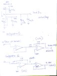
New Doc 2017-05-01_1.jpg

Kindly suggest which would be the best suitable configuration to avoid any effects of non linearity or impedance mismatch.
 
Last edited:

Hi pradhan.rachit,

I think you will face a trade-off between linearity and noise performance: if you use the amplifier in the first stage, you will have better noise performance but since the buffer sees an amplified signal its linearity may degrade. Putting the buffer at the first stage, the noise of the buffer may be a problem.

By the way, why do you need the buffer stage?

-Mahdi
 

Hi mahdi3999,

Thanks for the inputs. The datasheet suggests that the specifications of the Hall effect sensor are for 10k as the loading at the output.
The currents that will be sensed will be DC in nature, but the direction of the current will change as per the state of charge of the battery (Whether charging or discharging).

Also, what would be the best position to place an RC Low Pass Filter in this network?

- Rachit
 

The datasheet suggests that the specifications of the Hall effect sensor are for 10k as the loading at the output.

It seems that, putting the buffer in the first stage, you will not have a 10k load for the sensor, right?


Regarding the RC filter, if we only take the noise and linearity performance into account, the RC filter will not affect linearity (because it is implemented with passive and linear components). So you can put it at the end of the chain so that its noise becomes negligible.

-Mahdi
 

Both amplifier schematics are equally flawed. You designed a latch by applying positive feedback.

Besides amplifying HAIS 50 output by factor of two, you also need to shift the voltage range to useable PIC24F ADC input range, e.g. 0 - 3.3V. Typically the 2.5V midscale will be shifted to 1.5 or 1.65 V.
 
It seems that, putting the buffer in the first stage, you will not have a 10k load for the sensor, right?


Regarding the RC filter, if we only take the noise and linearity performance into account, the RC filter will not affect linearity (because it is implemented with passive and linear components). So you can put it at the end of the chain so that its noise becomes negligible.

-Mahdi

I'm planning to place the 10k load resistor at the input of the buffer. It will beat the purpose of having an high input impedance offered by the buffer, but the loading characteristics would be as per the datasheet. I am wondering if the RC Filter will drop any voltage accross it if it is placed after the buffer and amplification? If the impedance offered by the RC filter is close to that of the ADC's internal impedance, will it cause any sort of loading issues? If yes, how could it be avoided?

Both amplifier schematics are equally flawed. You designed a latch by applying positive feedback.

Besides amplifying HAIS 50 output by factor of two, you also need to shift the voltage range to useable PIC24F ADC input range, e.g. 0 - 3.3V. Typically the 2.5V midscale will be shifted to 1.5 or 1.65 V.

Thanks for pointing that out, FvM. I'll make the corrections in the schematic. I am using a PIC24FV32KA304 for control, which is a 0 - 5.5V MCU. Out of curiosity, what is the best way to level shift the reference voltages to lower levels in such systems, where the reference offered is 2.5V wheras the sensing midpoint needs to be around 1.65V?
 

Hi,

to simplify the whole circuit: I´d just overdrive the HAIS-50 VRef signal with 1.65V.
Use the ADC_VRef to generate the HAIS_VRef. Resistive voltage divider, smooting capacitor, OPAMP as buffer.

Then feed the HAIS-50 OUTPUT (with the recommended C) directely to the ADC.

Klaus
 

Hi,

to simplify the whole circuit: I´d just overdrive the HAIS-50 VRef signal with 1.65V.
Use the ADC_VRef to generate the HAIS_VRef. Resistive voltage divider, smooting capacitor, OPAMP as buffer.

Then feed the HAIS-50 OUTPUT (with the recommended C) directely to the ADC.

Klaus

Keeping simplicity out of the consideration, can you tell how has the performance of the system been in the configuration that you specified?
 

Hi,

* no additionally introduced gain errors
* lowest possible offset and offset_drift error
* resolution: 64.4mA/LSB at 3.3V full_scale (best resolution is 24.4mA/LSB)

--> if you want to calculate charge (Ah, As) then I assume the reduced offset gives more precision than you loose because of the reduced resolution.

* offset errors integrate over time to a big error
* resolution error cancels out by integration over time (depending on signal noise, ADC performance, signal level)

Klaus
 
Thank you KlausST.

I think the offset drift error is going to be of maximum concern through the life of the product. I am considering of overriding the reference to 1.65 V in the system.

Hi,
* resolution error cancels out by integration over time (depending on signal noise, ADC performance, signal level)

Klaus

I didn't understand the quoted point. Can you please elaborate?
 

Are you measuring AC or DC current ?
I've done it on DC with an 60A 60mV shunt and an op-amp set up as a differential mode, The output from the op-amp is fed via a 2.50V reference voltage fed through 2K resistors, so when nothing is running through the shunt it reads half the reference voltage 1.24950V (off set so it reads 0.00A on LCD with nothing connected)then depending which way the current flows through the shunt in either direction it either adds or subtracts from the 1.24950V. This is then fed into a MCP3426 (16bit A/D converter) with accurate results. See Pic below, Still needs a bit of tweaking to get even better results but I'm happy with the readings so far. I need to run a 30amp load through it to check the top end. But this is only for DC current.
meter.JPG
 
Hi,

"depending on signal noise, ADC performance, signal level"

Assume you have a very clean signal, noise far below one LSB, the ADC works with noise below one LSB...
Then the most extreme error could be 1/2 LSB, which is about 32mA (or about 12mA).
Now integrate this error over time and get 1Ah in about 30h (80h)
(Mind that this is an extreme and thus not realistic view)

But if your total noise is larger than one LSB, then the error toggles. The error will be positive and negative. Now integrate this and you will see that the overall error will cancel out over time.

Real world will be somewhere between those extremes.

In some cases one adds some analog "noise" (dither) to a very clean system to avoid that the error can integrate over time.

Klaus

- - - Updated - - -

Added:
(I've just read wizpic's post)
If you want to do intelligent charge calculation of a battery, then I recommend:
* integrating charging (positive) current over time (multiplied with charging efficiency)
* integrating discharging (negative) current over time
Then you are able to compensate for charging efficiency. And you may add self discharge calculations.


Klaus
 
Sorry I've just re-read topic and seen it's DC you are measuring. If you wanted to have a look at this route with shunt and op-amp I could get my schematic completed. I was thinking about building a battery monitor and using this current sense circuit so it can measure current in and out of the battery but not quite got around to doing to much work on it yet.
 

Here is my schematic of the current measurement part, This was part of a wireless meter I did but measuring voltage but just used the PCB, changed couple of resistors and code to measure current. Has you can see IC1 is set up in differential mode,R5&R7 divide the 2.50V reference in half so it can read voltage in either direction, This is then read by the MCP3426 and captured this then sets the 0.00 value. It displays a minus sign if it goes 0.00A. The voltage version of this can measure 0-99.99V which ever way the input leads are connected as it runs of a battery so it's isolated with great results. I've just done the modification to read current and it's in the early stage of the design.
I need to look at the input filters in more detail as this is new part of the design, But by hooking it up and adding it to it, it seems to improve the readings so may add it or not yet.
By all means if the design could be improved I'm open to suggestions.
current.PNG
 

Hi,

The circuit seems not bad.

I see some possible modifications that ease the design and at the same time make the measurement more precise.
But I'm in hurry now. It takes a couple of hours..I'll be back

Klaus
 

Hi,

The circuit seems not bad.

I see some possible modifications that ease the design and at the same time make the measurement more precise.
But I'm in hurry now. It takes a couple of hours..I'll be back

Klaus
Thanks I will wait before I lay out the PCB, So if the design can be improved or made easier to make then I'll wait and try new suggestions

Sorry did not mean tp highjack topic :)
 

Hi wizpic, thanks for sharing your schematic.

Can you specify the reason for selecting the filter cutoff frequency as 10 Hz?
 

To be honest I found it from the web some where, At the time I was using an AD1115 (16bit) breakout board and was not 100% happy with the results so I did a bit of searching and came across the filter, The reply was that it cure/made the readings better, I wanted to avoid the dirty averaging method in software. I just tired it and the readings became more stable and better. Plus I'm working on a project measuring and Angle sensor and a pressure transducer taking 40 samples for second(well more than really) I send out 40 samples to an SD card. Adding the filter made the readings more stable. I'm currently doing some research into how or why it does to get a better understanding of it.
 

Hi,

* I often use low pass filtering as early as possible in the signal flow. This prevents voltage spikes on the signal inputs to cause problems. Fc should be well below bandwidth of the Opamps, but could go down to your 10Hz. Here I recommend fc to be below 10kHz. At least 2.2nF across R1 and 2.2nF across R8.

* Adding offset.
It's more easy to add the offset at the difference amplifier circuit. Therefore I'd replace R8 (10k) with two 20k resistors. One goes to GND, the other to 2.5V reference voltage. The resulting resistance is still 10k, while it adds 2.5V/2 as bias voltage to the output.
Now you may omit IC4 completely. This additionally "omits" the introduction of the errors of IC4 (noise, offset, offset drift).
Another benefit is that the signal output is low impedance.
If you further want to simply improve signal performance, then replace R1 with two paralleled 20k. This decreases thermal offset drift of the difference amplifier circuit.

Reference, offset.
The best way to add constant offset to the circuit is to use the same Vref as the ADC. Because the ADC lacks of VRef input and output this is not possible with your circuit.

Filter.
Each ADC should have an anti aliasing filter at the analog signal input. Therefore your filter is good. If you see the frequency response chart of the ADC, then you see the overall attenuation of a 10Hz signal is not very good. About 6dB in the ADC and 3dB in your filter.
But it's OK

ADC input:
The source impedance for the ADC input is worst at DC. It is about 110kOhms. As your expected signal frequency is near DC...you may expext measurement errors (gain, but also offset, offset drift, and depending on ADC input circuit: channel crosstalk, too).
Therefore I recommend to use a lower impedance filter. Maybe 1k, 10uF, 10k, 1uF.
The ADC input is a switched capacitor. This causes high current peaks. Therefore I recommend to put the last filter capacitor (my 1uF, or 100nF in your circuit) as close as possible to the ADC input. Use a ceramic one, no electrolytic.

Voltage measurement path:
I'd reduce part count. Omit R10 and R13. Use the same Cs as in the current path filter. To keep about the same gain as in your circuit I recommend: 47k, 1k2, 10uF, 10k, 1uF.

Negative supply voltage.
This is switched capacitor technique, it generates a lot of noise. I recommend to add an additional RC filter at the output: 10R, 10uF.

All in all only minor changes. Not a single one is a "must" in my eyes.

Klaus
 
  • Like
Reactions: wizpic

    wizpic

    Points: 2
    Helpful Answer Positive Rating
Thank you Klaus,
This makes interesting reading, I shall take on board your comments and certainly will be trying them on the design I have set up no in my workshop.
One of the reasons I went for 2.5Vref is that the MCP3426 as it's own Vref of 2.048V(which is its max input) and dividing the 2.5V by half this gives me 1v to play with either side, The ADS1115 can go up to 4.096V input as my PCB'S are made for the MCP3426 I'll do the testing on this one, Then as well as with the ADS1115 version which I've mocked up based on the same design.
If I have any questions I think it may be best to start a new thread rather than highjack this thread if that's ok with you ?
Once again thanks for your help

Wizpic
 

Status
Not open for further replies.

Part and Inventory Search

Welcome to EDABoard.com

Sponsor

Back
Top